 |
 |
| How
many transistors can dance on the head of a chip only 118 millimeters
square? Over 58 million, thanks to IBM’s sophisticated process
technology that builds them just 130 nanometers wide. Such superior
technology developments turbo-charge the G5 processor to speeds of up
to 2GHz. To get electronics so small requires miniaturization breakthroughs, and IBM’s dedication to basic scientific research makes these advances possible. For instance, the company began researching copper as an interconnect method over 25 years ago, but the technique wasn’t practical until just recently.
Transistors on the PowerPC G5 hold a charge to let the system make logic decisions based on whether the transistor is on or off. IBM builds these devices just .00000013 meters wide on a layer of silicon on insulator. The 58 million transistors themselves are connected by over 400 meters of copper wire that’s less than 1/800th the width of a strand of your hair. Tiny paths mean less time to complete a sequence, since the electrons don’t need to travel as far. In other words, the PowerPC G5 is fast. Silicon on Insulator (SOI) refers to placing a thin layer of silicon on top of an insulator, such as silicon oxide or glass. The transistors are then built on top of this thin layer of SOI, reducing the capacitance of the switch. Reducing capacitance lets the switch operate 20-35% faster than bulk fabrication technology, and that’s nothing to sneeze at. But it’s only half the picture.
Smaller transistors increase the difficulty of wiring them together. For over 30 years, the semiconductor industry relied on aluminum wiring to connect transistors. But as semiconductors get smaller, requiring thinner and narrower connections, aluminum gets harder and harder to use, as it resists the flow of electricity. And at such small sizes, resisting electrons may even jump wires, turning nearby transistors on and off when they aren’t supposed to. Translation: less predictability, less reliability. At these microscopic sizes, copper transmits electrical signals faster than aluminum, and more reliably. IBM’s additive-copper, dual-damascene wiring process replaces the conventional subtractive-aluminum process. The damascene method isn’t new — swords made in Damascus, Syria over 2,500 years ago were forged with this process. The rest of the industry has utilized the damascene process for copper circuit boards, but IBM was the first company to discover a method that allows copper to be used in chip wiring. The result is a 40% gain in conductivity and a further boost in processing performance. |
Tools of
the Trade As the metallurgy for the new millennium, intricate electronics in today’s processors call for clean-room technology. IBM’s 130-nanometer complementary metal-oxide semiconductor (CMOS) process requires the precision motion of 21st century robots.  Swell
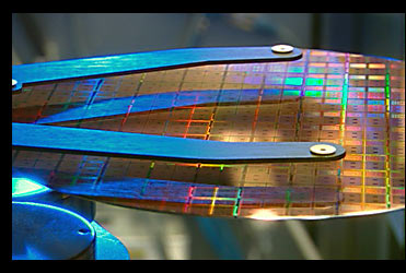
FOUPs. At IBM’s state-of-the-art 300-mm chip fabrication facility
in East Fishkill, NY, front opening unified pods (FOUP) hold silicon
wafers during various stages in a weeks-long process. FOUPs travel
along the factory ceiling via Sky-Rav, never exposing their precious
cargo to the outside air. Swell
FOUPs. At IBM’s state-of-the-art 300-mm chip fabrication facility
in East Fishkill, NY, front opening unified pods (FOUP) hold silicon
wafers during various stages in a weeks-long process. FOUPs travel
along the factory ceiling via Sky-Rav, never exposing their precious
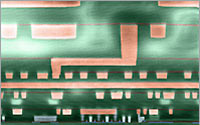
cargo to the outside air. Spin Cycle. A critical stage in the
process, one tool dispenses a layer of photo-resist material onto a
spinning wafer, distributing it evenly. At the next stage, a camera
hardens the material around a mask. Then other tools rinse away the
material not hardened, which leaves a channel for the metal. Spin Cycle. A critical stage in the
process, one tool dispenses a layer of photo-resist material onto a
spinning wafer, distributing it evenly. At the next stage, a camera
hardens the material around a mask. Then other tools rinse away the
material not hardened, which leaves a channel for the metal.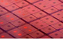 Mightier Than the Sword. The damascene process
creates a hole, which is then filled with material and polished to
remove excess metal, as opposed to a subtractive process in which one
deposits aluminum, and then etches away metal that isn’t part of the
design. Mightier Than the Sword. The damascene process
creates a hole, which is then filled with material and polished to
remove excess metal, as opposed to a subtractive process in which one
deposits aluminum, and then etches away metal that isn’t part of the
design. |

| . | . | . |
| -- |
PowerMac G5
|
Juli. |
|
- |
64-bit breakthrough
|
2003
|